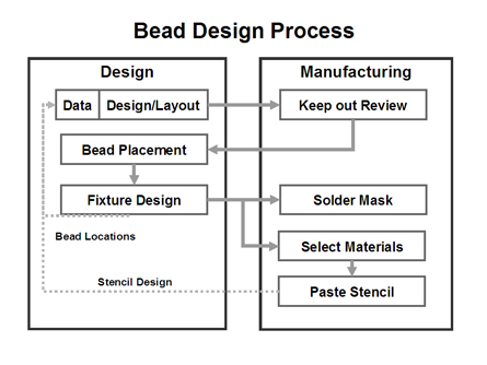
TestSight Developer’s Bead Design functionality is the first software package to provide fully automatic bead probe placement and editing, as well as integrated Paste Stencil and Solder Mask design. Developer’s Bead Design conforms to the design rules specified in the Keysight Medalist Bead Probe Handbook, and provides accurate calculations for the Paste Stencil and Solder Mask size designs.
The Bead Design placement algorithm automatically determines the location and angle of beads on all traces, blind vias or micro-pads. Spacing from other pads and trace corners is determined automatically using pre-set values. Bead Design also protects against sizing and placing beads where mask registration errors can cause bead deformation.
Bead Keepout and Layer Cutdown (thickness) areas can be easily defined using graphical editing tools.
The critical design values for a successful bead project include the Paste Stencil size and the Solder Mask opening. The Paste Stencil size determines the amount of metal deposited on a bead. Too much or too little metal can lead to contact reliability problems. Bead Design uses all the variables that affect the metal volume, including the Print Area Ratio (PAR), the Paste Transfer Ratio (TR), the Solder Paste Metal ratio, and the layer thickness.
Bead Design provides a powerful before-and-after analysis tool that lets the user immediately determine the impact of using beads on In-Circuit Test contact coverage.